Advanced Optical Integration Processes for Photonic‐Integrated
In response to these demands, device packaging developments have focused on achieving compactness, high efficiency, and high performance. Photonic integrated chip packaging
3-D Packaging Technologies for Advanced Integrated Photonics
Recent developments in photonics applications, in the fields of datacom, high-performance computing, and integrated optical sensors, have accelerated the trend toward
Establishing a Packaging Ecosystem for
Passively place InP laser in laser trench using fiducial marks Laser placement on SiPh chip has potential to significantly reduce packaging costs for Datacom, LiDAR & photonic computing applications
Advanced Semiconductor Packaging | Silitronics
Silitronics delivers advanced semiconductor packaging, silicon photonics, design, fabrication, and assembly solutions for high-performance applications.
Automated, high-throughput photonic packaging
Silicon photonics can enable optical circuits of unprecedented complexity and cost efficiency. It employs lithography to effectively pre-assemble optical devices on wafers fabricated in
Integrated Photonics Packaging
Packaging and assembly technologies are critical to making devices available for high-volume, low-cost applications. This includes heterogeneous and hybrid integration: the dense integration of compound
Advanced Packaging for Silicon Photonics: Techniques, Business
Advanced packaging techniques offer innovative solutions to overcome these limitations by providing denser interconnections, shorter signal paths, and improved thermal management for
Electronic Chip Package and Co-Packaged Optics (CPO) Technology
The 2.5D packaging approach uses interposers to connect multiple chips, including silicon photonics chips, effectively increasing interconnection density, reducing chip area, and lowering
Advanced Packaging Evolution: Chiplet and Silicon Photonics-CPO
ASE has introduced a Silicon Photonics packaging platform designed to deliver innovative solutions that facilitate more advanced AI systems while ensuring high performance and energy efficiency.
Photonics Packaging and Systems Integration
Explore Tyndall''s advanced photonics packaging technologies and systems integration. Learn about our cutting-edge research in optical interconnects, silicon photonics, and more.
Telecom Racks & Cabinets
19-inch racks, wall-mount cabinets, open frames with high load capacity and seismic rating.
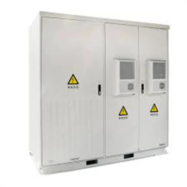
Outdoor Climate Cabinets
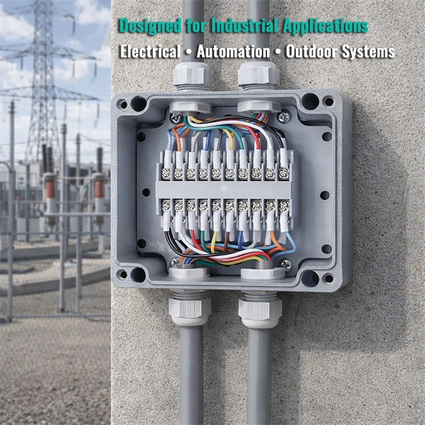
IP55/IP66 outdoor enclosures with integrated cooling/heating, -40°C to +55°C operation.
Smart PDUs & Power Distribution
Intelligent PDUs with remote monitoring, per-outlet switching, and environmental sensors.
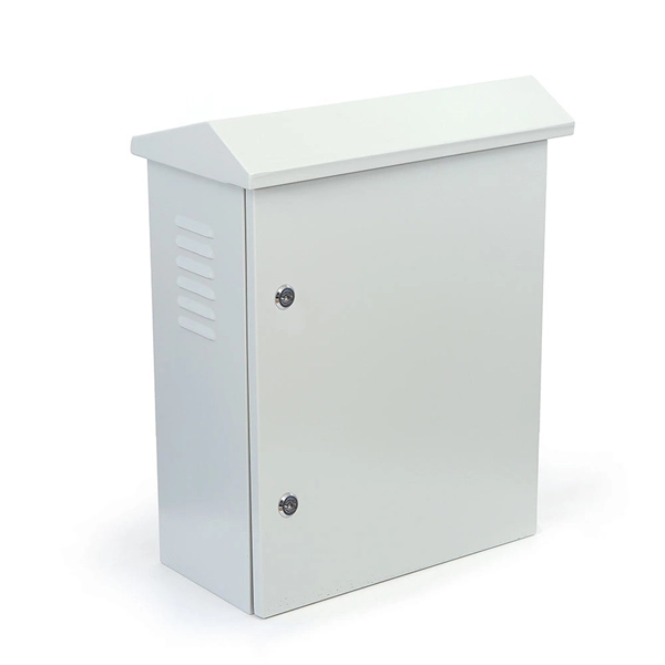
Shelters & Network Cabinets
Prefabricated telecom shelters, emergency comms shelters, and network cabinets with cable management.